- 您现在的位置:买卖IC网 > Sheet目录1228 > MAX5980EVKIT# (Maxim Integrated Products)EVAL KIT MAX5980
�� �
�
�Quad,� IEEE� 802.3at/af� PSE� Controller�
�for� Power-over-Ethernet�
�Slave� Address�
�The� device� has� a� 7-bit� long� slave� address� (Figure� 9).� The�
�bit� following� the� 7-bit� slave� address� (bit� eight)� is� the� R/� W�
�bit,� which� is� low� for� a� write� command� and� high� for� a� read�
�command.� The� upper� five� bits� of� the� slave� address� can-�
�not� be� changed� and� are� always� [01000].� Using� the� AD0�
�input,� the� lowest� two� bits� can� be� programmed� to� assign�
�the� device� one� of� four� unique� slave� addresses� (see�
�Table� 3).� The� device� monitors� the� bus� continuously,� wait-�
�ing� for� a� START� condition� followed� by� the� device’s� slave�
�address.� When� a� device� recognizes� its� slave� address,�
�it� acknowledges� and� is� then� ready� for� continued� com-�
�munication.�
�Global� Addressing� and� the� Alert� Reponse�
�Address� (ARA)�
�The� global� address� call� is� used� in� write� mode� to� write� to�
�the� same� register� to� multiple� devices� (address� 60h).� The�
�global� address� call� can� also� be� used� in� read� mode� (61h)�
�in� the� same� way� as� the� alert� response� address� (ARA).�
�The� actual� alert� response� address� (ARA)� is� 0Ch.� The�
�MAX5980� slave� device� only� responds� to� the� ARA� if� its�
�INT� (interrupt)� output� is� asserted.� All� MAX5980� devices� in�
�which� the� INT� output� is� not� asserted� ignore� the� ARA.�
�When� responding� to� the� ARA,� the� device� transmits� a�
�byte� of� data� on� SDAOUT� containing� its� own� address� in�
�the� top� 7� bits,� and� a� 1� in� the� LSB� (as� does� every� other�
�device� connected� to� the� SDAIN� line� that� has� an� active�
�interrupt).� As� each� bit� in� the� byte� is� transmitted,� the�
�device� determines� whether� to� continue� transmitting� the�
�remainder� of� the� byte� or� terminate� transmission.� The�
�device� terminates� the� transmission� if� it� sees� a� 0� on� SDA�
�at� a� time� when� it� is� attempting� to� send� a� 1;� otherwise� it�
�continues� transmitting� bits� until� the� entire� byte� has� been�
�sent.� This� litigation� protocol� always� allows� the� part� with�
�the� lowest� address� to� complete� the� transmission,� and� the�
�microcontroller� can� respond� to� that� interrupt.� The� device�
�deasserts� INT� if� it� completes� the� transmission� of� the�
�entire� byte.� If� the� device� did� not� have� the� lowest� address,�
�and� terminates� the� transmission� early,� the� INT� output�
�remains� asserted.� In� this� way,� the� microcontroller� can�
�continue� to� send� ARA� read� cycles� until� all� slave� devices�
�successfully� transmit� their� addresses,� and� all� interrupt�
�requests� are� resolved.�
�General� Call�
�In� compliance� with� the� I� 2� C� specification,� the� device�
�responds� to� the� general� call� through� global� address� 30h.�
�Message� Format� for� Writing� to� the� MAX5980�
�A� write� to� the� device� comprises� the� device� slave� address�
�transmission� with� the� R� W� bit� set� to� 0,� followed� by� at�
�least� 1� byte� of� information.� The� first� byte� of� information�
�is� the� command� byte� (Figure� 10).� The� command� byte�
�determines� which� register� of� the� device� is� written� to� by�
�the� next� byte,� if� received.� If� the� device� detects� a� STOP�
�condition� after� receiving� the� command� byte� but� before�
�receiving� any� data,� then� the� device� takes� no� further�
�action� beyond� storing� the� command� byte.�
�Any� bytes� received� after� the� command� byte� are� data�
�bytes.� The� first� data� byte� goes� into� the� internal� register�
�of� the� device� selected� by� the� command� byte� (Figure� 11).�
�The� control� byte� address� then� autoincrements� (if� pos-�
�sible;� see� Table� 4)� and� then� waits� for� the� next� data� byte�
�or� a� STOP� condition.�
�MSB�
�LSB�
�If� multiple� data� bytes� are� transmitted� before� a� STOP� con-�
�SDA/�
�SDAIN�
�0�
�1�
�0�
�A3�
�A2�
�A1�
�A0�
�R/W�
�ACK�
�dition� is� detected,� these� bytes� are� stored� in� subsequent�
�MAX5980� internal� registers� as� the� control� byte� address�
�SCL�
�autoincrements� (Figure� 12).� If� the� control� byte� address�
�can� no� longer� increment,� any� subsequent� data� sent� con-�
�tinues� to� write� to� that� address.�
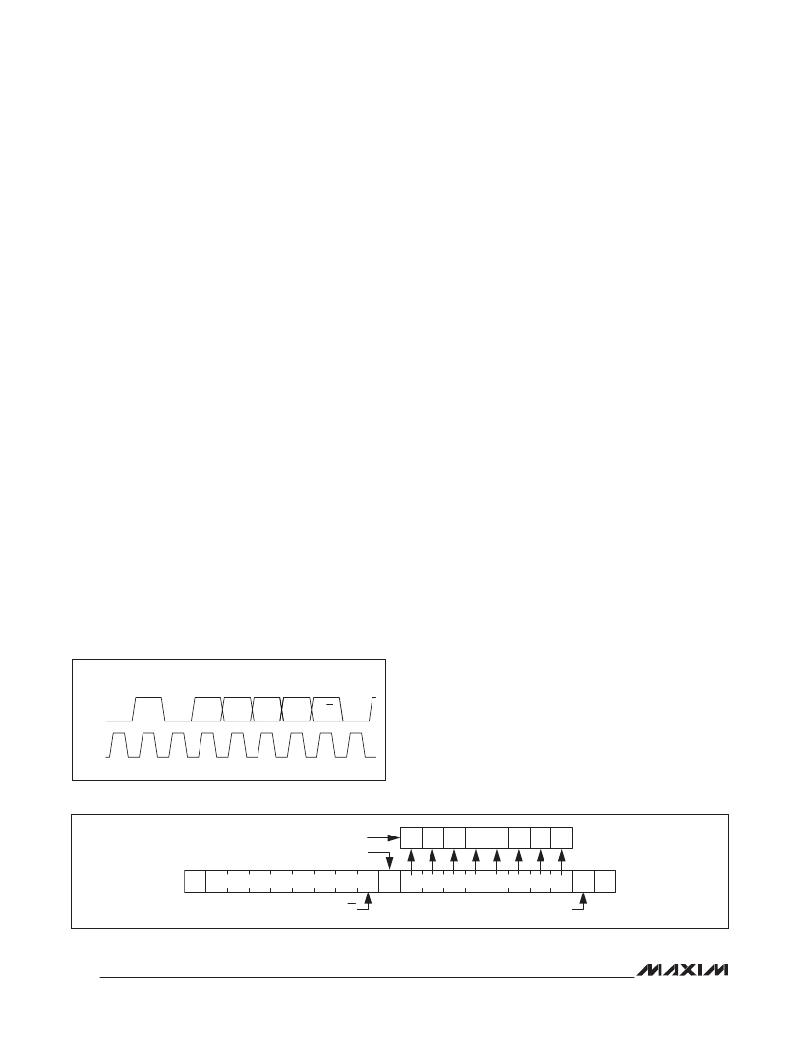
�Figure� 9.� Slave� Address�
�CONTROL� BYTE� STORED� ON� STOP� CONDITION�
�ACKNOWLEDGE� FROM� THE� MAX5980�
�CB7� CB6� CB5� CB4� CB3� CB2� CB1� CB0�
�S�
�SLAVE� ADDRESS�
�0�
�ACK�
�CONTROL� BYTE�
�ACK�
�P�
�Figure� 10.� Write� Format,� Control� Byte� Received�
�24�
�R/W�
�ACKNOWLEDGE� FROM� THE� MAX5980�
�发布紧急采购,3分钟左右您将得到回复。
相关PDF资料
MAX5982CEVKIT#
EVAL KIT MAX5982C
MAX6397SATA+T
IC SW OVERVOLT PROT 8-TDFN
MAX6496EVKIT+
KIT EVAL FOR MAX6496
MAX6651EVKIT
EVAL KIT FOR MAX6651
MAX7325EVKIT+
KIT EVAL FOR MAX7325
MAX7326EVKIT+
KIT EVAL FOR MAX7326
MAX7359EVKIT+
KIT EVAL FOR MAX7359
MAX7443EVKIT+
KIT EVAL FOR MAX7443
相关代理商/技术参数
MAX5980EVKIT+
功能描述:电源开关 IC - POE / LAN RoHS:否 制造商:Fairchild Semiconductor 开关数量:Single 开关配置:SPST 开启电阻(最大值):7.3 Ohms 串话: 带宽: 开启时间(最大值):13 ns 关闭时间(最大值):20 ns 切换电压(最大): 工作电源电压:8 V to 26 V 最大工作温度:+ 125 C 安装风格:Through Hole 封装 / 箱体:TO-220F-6
MAX5980GTJ+
功能描述:电源开关 IC - POE / LAN 0-16V Hot-Swap Controller
RoHS:否 制造商:Fairchild Semiconductor 开关数量:Single 开关配置:SPST 开启电阻(最大值):7.3 Ohms 串话: 带宽: 开启时间(最大值):13 ns 关闭时间(最大值):20 ns 切换电压(最大): 工作电源电压:8 V to 26 V 最大工作温度:+ 125 C 安装风格:Through Hole 封装 / 箱体:TO-220F-6
MAX5980GTJ+T
功能描述:电源开关 IC - POE / LAN 0-16V Hot-Swap Controller
RoHS:否 制造商:Fairchild Semiconductor 开关数量:Single 开关配置:SPST 开启电阻(最大值):7.3 Ohms 串话: 带宽: 开启时间(最大值):13 ns 关闭时间(最大值):20 ns 切换电压(最大): 工作电源电压:8 V to 26 V 最大工作温度:+ 125 C 安装风格:Through Hole 封装 / 箱体:TO-220F-6
MAX5980UTJ+
功能描述:电源开关 IC - POE / LAN 0-16V Hot-Swap Controller RoHS:否 制造商:Fairchild Semiconductor 开关数量:Single 开关配置:SPST 开启电阻(最大值):7.3 Ohms 串话: 带宽: 开启时间(最大值):13 ns 关闭时间(最大值):20 ns 切换电压(最大): 工作电源电压:8 V to 26 V 最大工作温度:+ 125 C 安装风格:Through Hole 封装 / 箱体:TO-220F-6
MAX5980UTJ+T
功能描述:电源开关 IC - POE / LAN 0-16V Hot-Swap Controller RoHS:否 制造商:Fairchild Semiconductor 开关数量:Single 开关配置:SPST 开启电阻(最大值):7.3 Ohms 串话: 带宽: 开启时间(最大值):13 ns 关闭时间(最大值):20 ns 切换电压(最大): 工作电源电压:8 V to 26 V 最大工作温度:+ 125 C 安装风格:Through Hole 封装 / 箱体:TO-220F-6
MAX5981AETE+
功能描述:热插拔功率分布 IEEE 802.3af/at PDIC Controller
RoHS:否 制造商:Texas Instruments 产品:Controllers & Switches 电流限制: 电源电压-最大:7 V 电源电压-最小:- 0.3 V 工作温度范围: 功率耗散: 安装风格:SMD/SMT 封装 / 箱体:MSOP-8 封装:Tube
MAX5981AETE+T
功能描述:热插拔功率分布 IEEE 802.3af/at PDIC Controller
RoHS:否 制造商:Texas Instruments 产品:Controllers & Switches 电流限制: 电源电压-最大:7 V 电源电压-最小:- 0.3 V 工作温度范围: 功率耗散: 安装风格:SMD/SMT 封装 / 箱体:MSOP-8 封装:Tube
MAX5981AEVKIT#
制造商:Maxim Integrated Products 功能描述:EVKIT FOR POWERED DEVICE INTERFACE CONTROLLERS WITH INTEGRAT - Boxed Product (Development Kits) 制造商:Maxim Integrated Products 功能描述:KIT EVAL INTERFACE CONTROLLER